


Degradation phenomena of quantum dot light-emitting diodes induced by high electric field
*This article has been summarized for the purpose of providing shorter and more accessible reading. For the full original article, please go to https://doi.org/10.1088/1361-6528/acc871.
Introduction
Despite the successful commercialization of quantum dot light-emitting diodes (QLED) displays, there are still several issues that need to be addressed, particularly with respect to their lifetime and stability [5-9]. In particular, the degradation of a QLED induced by an electric field or current is a critical problem that hinders the commercialization of QLED devices based on electroluminescence (EL) [10]. The degradation issue under a high electric field can become more important as the dimensions of the devices reduce and the applied electric field effectively increases. One of the main causes of degradation in light-emitting devices is the indium thin oxide (ITO) layer, which is commonly used as a transparent conducting electrode, as the In and Sn ions from the ITO layer can migrate or diffuse through the device, especially under high electric fields [11-13]. Despite numerous efforts to study the degradation phenomena of QLED devices, systematic microscopic analyses have not been performed yet.
Scanning probe microscopy (SPM) and transmission electron microscopy (TEM) are powerful tools for investigating the properties of nanomaterials due to their excellent imaging resolution [1]. In particular, Atomic Force Microscopy (AFM), a type of SPM, is highly versatile and can be operated in various application modes, including Kelvin probe force microscopy (KPFM) [14]. In addition, a sharp AFM tip can be used to manipulate a sample surface or any nanostructures adsorbed on the sample surface with high precision [15].
In this study, we conducted a systematic analysis of the degradation of QLED devices induced by high electric fields, using a combination of SPM and TEM measurements. Initially, a local high electrical field was applied to the surface of a QLED device using an AFM tip in Contact mode. Changes in the morphology and work function (WF) were subsequently investigated in KPFM mode. Following the AFM experiments, TEM measurements were performed on the degraded sample area caused by the electric field of the AFM tip. Our results indicate that QLED devices can undergo mechanical degradation when exposed to high electric fields, resulting in significant changes in the work function within the degraded areas. Additionally, from the TEM When the electric field was applied, the surface was physically damaged and referred to as mechanical damage measurements, we observed the migration of In ions from the ITO bottom electrode and partial deformation of the ITO layer. The systematic approach we utilized in this study can serve as an effective methodology for investigating the degradation phenomena of various optoelectronic devices.
Materials and methods
Figure 1(a) shows the structure of the QLED device used in the study. The details of the preparation of the QLED device are described elsewhere [11]. Figure 1(b) shows the TEM images of dispersed QDs. Figure 1(c) is a photo from the sample area (dimensions 3 mm × 3 mm) containing the Al top electrode. Supplementary figure 2 shows the EL properties of a QLED device. The maximum luminance and current efficiency of the device were 30350 cd m-2 and 16.82 cd A-2, respectively.

Figure. 1. (a) The schematic of a QLED device structure. (b) The cross-sectional TEM image of the pristine QLED device without an Al top electrode. (c) When a positive voltage(red) is applied to the bottom electrode and a negative voltage(black) is applied to the top electrode, the QLED device emits light.
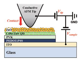
Figure. 2. The schematic of the surface manipulation method using a conductive AFM tip
Figure. 2 shows a schematic of the proposed method, in which the conductive AFM tip is used to induce local degradation of the QLED device through contact force and the applied electric field. AFM-based surface manipulation was performed on the sample areas without the Al top electrode using a Park Systems’ AFM instrument (NX10), as the conductive AFM tip serves as the top electrode. First, the sample surface was scanned in non-contact mode based KPFM mode. KPFM is a powerful AFM-based technique that simultaneously acquires surface potential maps (i.e., work function) and corresponding topographic images [27]. Second, appropriate sample and tip bias voltage were applied for 30 seconds. The tip was [MicroMasch, NSC36 Cr-Au lever A, resonance frequency: 90 kHz, force constant (k): 1 N/m] then brought into contact at only one point with the sample at a predefined contact-force. Third, the sample area was rescanned in KPFM mode to observe the changes in morphology and work function induced by the AFM-based surface manipulation. This process was repeated under various bias voltages or contact-forces to perform the AFM-based surface manipulation. After that TEM measurements were performed on the QLED sample areas exhibiting clear degradation features induced by the high electric field applied using the AFM tip, as well as on pristine sample areas.
Results and discussion
Figure 3. shows the results of the AFM-based surface manipulation of the QLED sample. The value of Vsample and Vtip were 10 V and -10 V, respectively, and the contact-force was 67.5 nN. Before contact, the sample surface was mostly flat, except for dust-like particles smaller than 300 nm, and the work function was nearly uniform without any specific features, as depicted in figures 3(a) and (b). After the AFM tip made contact with the sample under the aforementioned conditions, a distinct protrusion formed at the center of the sample area, as shown in figure 3(c). Furthermore, the work function map depicted in figure 3(d) indicates that the work function near the newly formed surface protrusion in the sample region was reduced compared to that in the surrounding region. The line profiles of the newly formed protrusion and the corresponding work function, extracted from the dashed line in figures 3(c) and (d), are shown in figure 3(e). The height of the surface protrusion was ~40 nm, and the work function was reduced by approximately 0.1 eV.
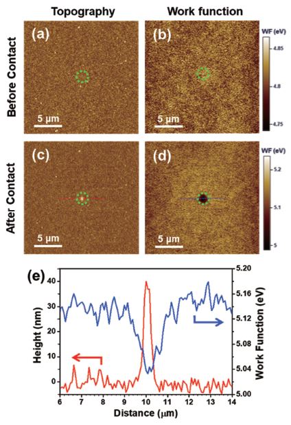
Figure. 3. Topographic (a), (c) and work function (b), (d) images of the QLED device without an Al top electrode before (a), (b) and after (c), (d) the AFM-based surface manipulation with Vsample = 10V, Vtip = -10Vand a contactforce of 67.5 nN. (e) Line profiles of the region indicated by the red and blue dotted lines in (c) and (d).
For a more systematic analysis, we carried out the AFM-based surface manipulation process repeatedly after adjusting the contact positions on the sample surface to parallel location and varying the contact conditions, such as Vsample, Vtip , and contact-force. Figure 4 presents the results of the repeated AFM-based surface manipulation for various Vsample and Vtip values. For this measurement, the contact-force was fixed at 67.5 nN. As shown in figures 4(c) and 4(d), the surface protrusion was newly formed and the work function was also lowered when ΔV, defined as Vsample -Vtip was equal 16 V since we clearly see protrusion and changed WF at +8V /-8V.
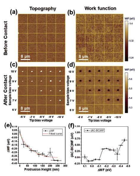
Figure. 4. Topographic (a), (c) and work function (b), (d) images of the QLED device without an Al top electrode before (a), (b) and after (c), (d) the repeated AFM-based surface manipulation for various (6 V, 7 V, 8 V, 9 V, 10 V) and (-6 V, -7 V, -8 V, -9 V, -10 V), and a fixed contact-fore of 67.5 nN. (e) A plot of the relationship between ΔWF and the protrusion height. (f) A plot of the relationship between After contact - Before contact (AC-BC)WF and ΔWF
A ΔV of 16 V indicates a considerably high bias voltage between the top and bottom electrodes of the QLED device, as the conductive AFM tip acts as the top electrode. The surface protrusion and work function reduction resulting from the AFM-based surface manipulation process were degradation features that were induced when a considerably high electric field was applied to the device. Additionally, the formation of the surface protrusions and lowering of the work function could be observed only when Vsample and Vtip were positive and negative, respectively. In the opposite condition, that is, when Vsample was negative and Vtip was positive, we could not observe any significant changes in the morphology and work function of the QLED sample surface. This finding indicates that the directionality of the bias voltage which can induce degradation features such as the protrusions and work function lowering. Through repeated surface manipulation, we obtained abundant data before and after degradation under diverse bias voltage conditions, and ΔWF was calculated by subtracting the work function in the pristine region from that in the degraded region. The relationship between the calculated ΔWF values and the heights of the newly formed protrusions is plotted in figure 4(e), which shows that ΔWF tends to decrease as protrusion height increases. Although the work function was lowered in the directly degraded region, the work function of the entire scanned area tended to increase after the AFM-based surface manipulation, which might have been caused by the surface-charging effect. The difference in the work function of the entire scanned area before and after the surface manipulation, designated as (AC-BC) WF, was also calculated. Figure 4(f) shows the relationship between (AC-BC)WF and ΔWF; (AC-BC)WF increased with increasing ΔWF. However, it was not a simple monotonic increase, and the QLED degradation seemed to occur in three discrete phases.
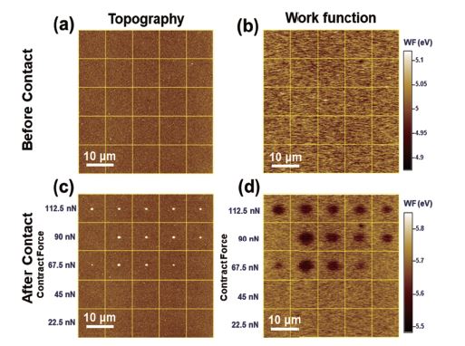
Figure. 5. Topographic (a), (c) and work function (b), (d) images of the QLED device without an Al top electrode before (a), (b) and after (c), (d) the repeated AFM-based surface manipulation for various contact-force (22.5 nN, 45 nN, 67.5 nN, 90 nN, 112.5 nN). Vsample and Vtip were fixed at 7 V and -7 V.
Figure 5. shows the results of the repeated AFM-based surface manipulation for different contact-force values ranging from 22.5 to 112.5 nN. The measurements were conducted with Vsample and Vtip values of 7 V and -7 V, respectively. As shown in figures 5(c) and (d), surface protrusions and work function lowering were observed only for the contact-forces larger than 67.5 nN. A lower contact-force indicates a higher contact resistance between the tip and sample. If the contact resistance increases, the bias voltage (or electric field) effectively applied through the QLED device decreases. Therefore, it is essential to set the contact-force at a sufficiently high level to minimize the contact resistance.
Lastly, TEM measurements were conducted on positions of the QLED sample where surface protrusions and work function reduction were observed after applying a high electric field. Figure 6 shows a typical cross-sectional TEM images acquired at the degraded position.

Figure. 6. (a) The cross-sectional TEM image of the pristine QLED device without an Al top electrode. (b) A cross-sectional TEM image of the QLED device that was degraded by the high electric field applied using the AFM-based surface manipulation process.
Conclusion
This study presented a systematic analysis of the degradation of a QLED device induced by high electric fields using SPM and TEM measurements. By applying a locally high electric field on the QLED sample surface in AFM Contact mode and investigating the changes in morphology and work function in KPFM mode, we observed severe mechanical degradation of the QLED device and significant changes to the work function in the degraded areas under high electric field conditions. TEM measurements confirmed the migration of metal ions from the ITO bottom electrode and partial deformation of the ITO layer. Our findings highlight the importance of investigating the degradation phenomena of QLED devices, and the systematic approach used in this study provides an adequate methodology for future research of various optoelectronic devices.
Reference
[1] Bayda S, Adeel M, Tuccinardi T, Cordani M and Rizzolio F2020 The history of nanoscience and nanotechnology: from chemical–physical applications to nanomedicine Molecules 25 112
[2] Choi M K, Yang J, Hyeon T and Kim D-H Flexible quantum dot light-emitting diodes for next-generation displays npj Flex. Electron. 2 10
[3] Yoon S H, Kim S, Woo H J, Kim J, Kim Y W, Seo S, Yoo E, Cho J, Song Y J and Choi Y J 2021 Flexible quantum dot light-emitting diodes without sacrificing optical and electrical performance Appl. Surf. Sci. 566 150614
[4] Ji W, Wang T, Zhu B, Zhang H, Wang R, Zhang D, Chen L, Yang Q and Zhang H 2017 Highly efficient flexible quantum-dot light emitting diodes with an ITO/Ag/ITO cathode J. Mater. Chem. C 5 4543–8
[5] Zhang X, Bao H, Chen C, Wu X, Li M, Ji W, Wang S and Zhong H 2023 The fatigue effects in red emissive CdSe based QLED operated around turn-on voltage J. Chem. Phys. 158 131101
[6] Chen S, Cao W, Liu T, Tsang S-W, Yang Y, Yan X and Qian L 2019 On the degradation mechanisms of quantum dot light-emitting diodes Nat. Commun. 10 756
[7] Chang J H et al 2018 Unraveling the origin of operational instability of quantum dot based light-emitting diodes ACS Nano 12 10231–9
[8] Xue X, Dong J, Wang S, Zhang H, Zhang H, Zhao J and Ji W 2020 Degradation of quantum dot light emitting diodes, the case under a low driving level J. Mater. Chem. C 8 2014–8
[9] Doe T et al 2021 Evaluation of degradation behavior in quantum dot light-emitting diode with different hole transport materials via transient electroluminescence Appl. Phys. Lett. 118 203503
[10] Yang J, Choi M K, Yang U J, Kim S Y, Kim Y S, Kim J H, Kim D-H and Hyeon T 2021 Toward
full-color electroluminescent quantum dot displays Nano Lett. 21 26–33
[11] Yoon S H et al 2019 Insertion of an inorganic barrier layer as a method of improving the performance of quantum dot light-emitting diodes ACS Photon. 6 743–8
[12] Scholz S, Kondakov D, Lüssem B and Leo K 2015 Degradation mechanisms and reactions in organic light-emitting devices Chem. Rev. 115 8449–503
[13] Lee S T, Gao Z Q and Hung L S 1999 Metal diffusion from electrodes in organic light-emitting diodes Appl. Phys. Lett. 75 1404–6
[14] Melitz W, Shen J, Kummel A C and Lee S 2011 Kelvin probe force microscopy and its application Surf. Sci. Rep. 66 1–27
[15] Kim M, Lee S, Lee J, Kim D K, Hwang Y J, Lee G, Yi G-R and Song Y J 2015 Deterministic assembly of metamolecules by atomic force microscope-enabled manipulation of ultra-smooth, super-spherical gold nanoparticles Opt. Express 23 12766–76


