


Imaging Ellipsometry: a Tool for Studying Microstructured Surfaces
Christian Röling1,2
11 Institute of Physical Chemistry, Georg-August-University Göttingen, Tammanstraße 6, 37077 Göttingen, Germany;
2Accurion GmbH, Stresemannstraße 30, 37079 Götingen, Germany
Imaging Ellipsometry
Imaging ellipsometry, combines the power of ellipsometry with optical microscopy. It achieves the highest lateral resolution in the field of ellipsometry and offers a very sensitive imaging technology for thin films. Typical application is the characterization of microstructured thin films. The ep4 is the latest microscopic imaging spectroscopic ellipsometer with unique measurement capabilities. It can provide real-time ellipsometric enhanced contrast images, and maps of the ellipsometric angles Δ and Ψ. These data can be transferred into d and the optical properties by computerized optical modeling.

Setup of an imaging ellipsometer including objective and 2D CCD.

Imaging spectroscopic ellipsometer nanofilm_ep4.
Microscopic Mapping
- Microscopic mapping offers the highest lateral resolution in the field of ellipsometry (down to 1 µm).
- Each pixel works as a single detector.
Optical Modeling
- Fitting of optical- and metrological parameters for ultrathin films.
- Effective medium approach (EMA) also offers information about chemical composition
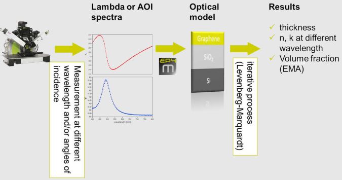
The Drude equation combines the reflection coefficients of p- (rp) and s-polarized (rs) with the ellipsometric angles Δ and Ψ. Hence rp and rs depend on complex refractive index and thicknesses of the investigated layers conclusions on n and k and thickness can be done. By varying wavelength and angle of incidence more independent values are obtained to improve the results.
Microcontact Printing
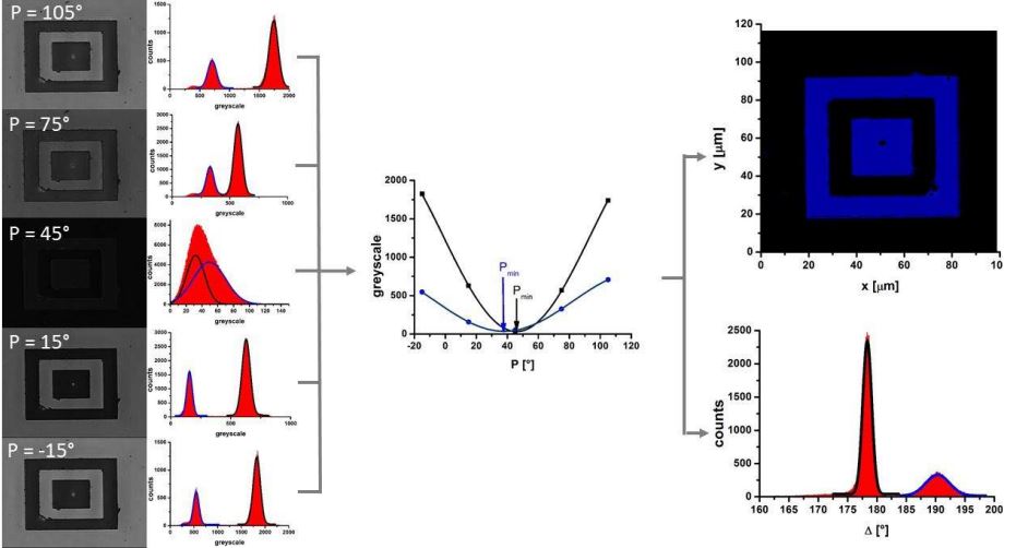
- Pattern of OTS on SiO2 surfaces by using microcontactprinting method on SiO surfaces [1].
- Fast recording of Δ-maps (λ = 658 nm, AOI = 50°) using 10x objective on 25 postions of 4 samples.
- Calculate Δ-maps into thickness-maps by interpolation using dispersion für SiO2 and Si(100) from database.
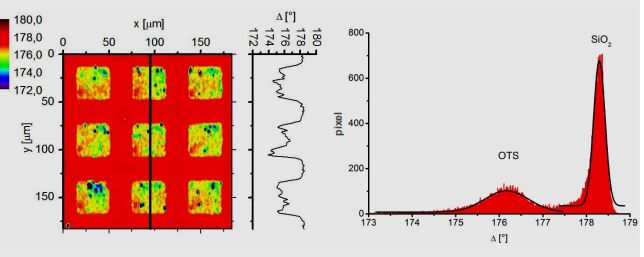
Left: Cropped Δ-map and line-profile of sample micropatterned with OTS (c = 5 mM) on SiO2/Si(100). Right: Correlating histogram of the Δ-map inclusive Gaussian fit for substrate and patterned SAM layer
- Quantitative study (n=100) of the pattern formation regarding the ink concentration.
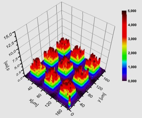
3D-plot of thickness-map (c (OTS)=5 mM) on SiO2/Si(100)
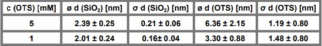
Results of quantitative histogram analysis (Gaussian Fit) of 100 thickness-maps varying the ink concentration.
Literature: [1] Kumar, Amit, Hans A. Biebuyck, and George M. Whitesides. "Patterning selfassembled monolayers: applications in materials science." Langmuir 10.5 (1994): 1498- 1511.
Laser Ablation
- Microstructured PMMA layer on SiO2/Si(100) formed by laser ablation (pulsed argon ion laser (λ = 193nm)).
- Variation in fluence and number of pulse by laser ablation on the sample.
- Recording Δ-maps (λ = 500 nm, AOI = 50°) using 50x objective on 12 postions of the sample.
- Calculate Δ-maps into thickness-maps by interpolation using dispersion for SiO2 , Si(100) and PMMA from database.
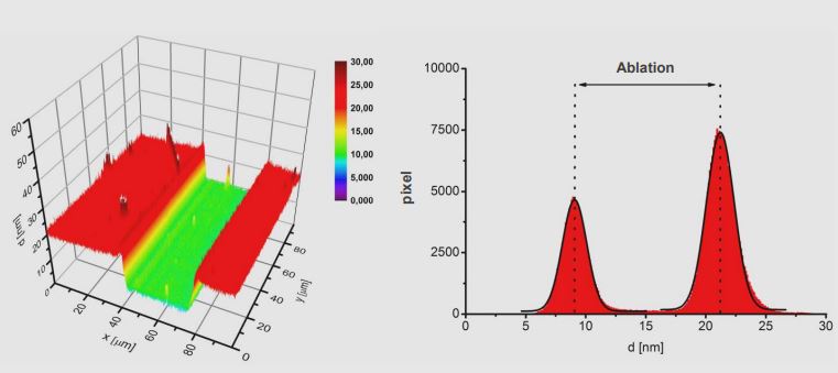
Left: d-map (3D-Plot) of microstructured thin PMMA layer (d = 21.9 nm) on SiO2/Si(100) Right: Correlating histogram of the thickness-map inclusive depth of ablation for PMMA using Gaussian fit analysis.
- Determination of the depth of ablation regarding fluence and number of pulse using Gauss Fit Histogram Analysis of thickness-maps.
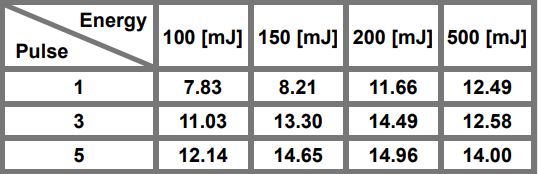
Calculated depth of ablation depending on pulse and energy obtained by histogram analysis of thickness-maps.
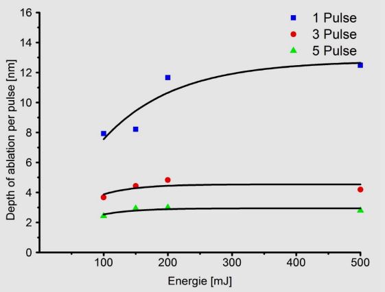
Exponential plot of the depth of ablation per pulse depending on the energy.
Holographic Interferometry
- Formation of photoinduced diffraction grating in amorphous As2S3 thin film on transparent subtrate by holographic interferometry [2]
- Mapping the photoinduced changes of refractive index (λ= 658 nm, AOI = 50°, 10x) regarding expose time.
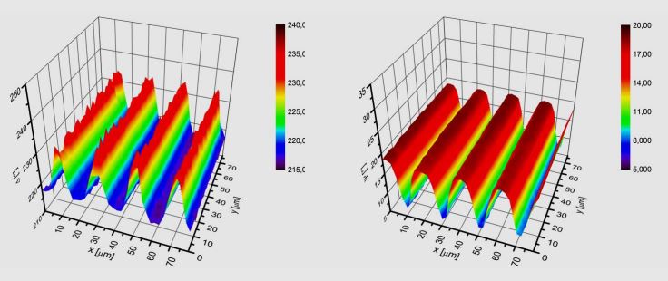
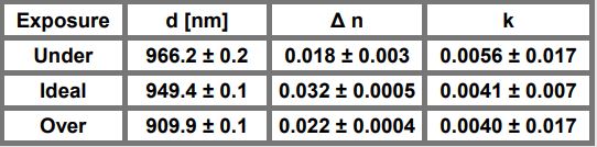
Δ-map (left) and Ψ-map (right) of microstructured amorphous As2S3 thin film on glass (d = 949.4 ± 0.1 nm) with proper-exposed gratings.
- Determine the thickness by Spectrosopic Ellipsometry (380-800 nm) using Tauc-Lorentz-Model.
- Calculate n+k values for each pixel using point to point method with fixed thickess (constant, measured by AFM).
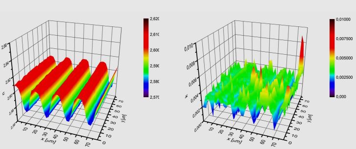
Obtained n-map (left) and k-map (right) of microstructured amorphous As2S3 thin film on glass (d = 949.4 ± 0.1 nm) with proper-exposed gratings.
- Gaussian Fit Analysis of n+k-maps regarding photoinduced changes in the optical parameters depending on the exposure time.
Results of quantitative histogram analysis of the n+k-maps with different exposure time.
Literature: [2] Röling, C., et al. "Imaging ellipsometry mapping of photo-induced refractive index in As2S3 films." Journal of Non-Crystalline Solids 365 (2013): 93-98.


